
A photonic chip workshop gives students a rare chance to hold difficult ideas in their hands: light, signals, materials, and design software, all gathered into a small engineered system. The best evidence from 2026 is not a sweeping claim that brief programs can solve workforce shortages. It is narrower and more useful: students can be introduced to optics, electronics, and AI-assisted design through structured lab activities, but the educational value depends on supervision, equipment access, and honest discussion of limits.
What A Photonic Chip Workshop Can Teach
Photonic Chip Workshop Skills Students Can See
A strong program begins with what students can observe. Light is a stern teacher. It does not care whether a student is confident; it bends, couples, scatters, and vanishes according to physical rules. That makes photonics useful for education. Students can see that engineering is not only a drawing on a screen. It is a repeated bargain among physics, fabrication, packaging, measurement, and cost.
The research notes point to programs where students worked with optics, fiber splicing, electronics, and engineering projects. Those activities matter because they place abstract chip design near the bench. A student who has seen how an optical fiber must be aligned will understand, more deeply than from a slide, why photonic components demand precision. A student who has built or tested an electronic circuit will have a better starting point for asking how electronic and photonic systems meet.
A photonic chip workshop should not promise that students will become chip designers in a weekend. That would be a poor bargain with the truth. Instead, it can teach the shape of the work: how design choices affect measurement, how lab practice affects data, and how AI tools may assist design without replacing the need to understand the underlying physics.
Evidence From 2026 Student Programs
What The CREOL Camp Shows
The clearest public example in the research is the CREOL Laser & Photonics Summer Camp, held in July 2026. According to CREOL, the program brought together more than 50 high school students from Florida, Ohio, and Mexico, with activities in optics, fiber splicing, electronics, and engineering through lab-based projects CREOL camp report. That scale is meaningful for outreach: large enough to suggest institutional planning, but still small enough that the setting likely depended on guided access to equipment and staff.
The evidence supports a practical claim: hands-on photonics education is already being offered to secondary students in organized university settings. It does not prove long-term outcomes such as college major choice, retention in engineering, or later employment. Those would require follow-up data. The camp record is a starting signal, not a settled verdict.
What The ASU Project Adds
Arizona State University reported in June 2026 that assistant professor Jiaqi Gu received a National Science Foundation CAREER Award to build an open-source electronic-photonic design automation, or EPDA, ecosystem. The ASU description connects education and research and frames the work as a way to make photonic chip design more accessible while combining physics, optics, electronics, and AI ASU News report.
This matters for a photonic chip workshop because AI-designed components are not only a hardware topic. They also depend on software, modeling, and design rules. If students only handle a polished chip, they may see technology as magic. If they only use software, they may miss the physical discipline of fabrication and testing. The ASU work points toward a bridge: design tools that can be taught in relation to the physical behavior of photonic devices.
AI Design Tools And Their Limits
Why AI Belongs In The Room
AI-assisted design can be introduced carefully. In an educational setting, students might compare a human-designed layout with an AI-assisted design exercise, then ask what the model optimized and what it ignored. The point is not to crown the algorithm. The point is to teach students to question outputs: What assumptions went into the model? What physical constraints were included? What measurements would test whether the design worked?
The ASU project is described as an effort to build an open-source EPDA ecosystem, not as a finished commercial product in the research notes. That distinction is important. A workshop can discuss open tools and research aims, but it should avoid treating early-stage educational infrastructure as if it were already standard practice across classrooms or industry.
Where Evidence Is Still Thin
The research does not provide controlled studies comparing students who attended these programs with students who did not. It does not give per-student costs for a camp, the number of trained instructors needed per lab group, or long-term safety and access requirements across different school districts. Those absences are not flaws in the programs; they are limits on what a reporter or educator should claim.
For a photonic chip workshop, this means success should be measured modestly. Did students learn key vocabulary? Could they explain why photonic design involves both optics and electronics? Did they understand why AI-generated designs still require physical testing? Did they practice safe, supervised lab habits? These are reasonable questions. Grand predictions are not.
Workshop Design For Student Learning
Building From Concept To Application
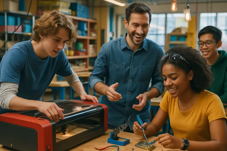
A well-planned session can be structured like a field notebook. First, students meet the concept: photonic chips use light in engineered components, and AI can assist parts of design. Next, they work with a visible demonstration in optics or electronics. Then they use a simplified design activity. Last, they connect the design to an application, such as AI-related computing hardware or optical communication, while clearly marking which parts are classroom models and which parts belong to advanced research or industry settings.
This progression matters because photonic chip components are small, often invisible to the unaided eye, and easy to romanticize. Students need anchors: a fiber, a circuit, a simulation, a measurement, a failed alignment. The failed alignment may teach more than the clean diagram. It shows that engineering is not a string of perfect answers, but a disciplined argument with matter.
- Start With Observation: Use safe optics and electronics demonstrations before asking students to interpret AI-assisted designs.
- Name The Boundaries: Tell students which activities are models, which are lab-tested, and which are still research-stage.
- Require Evidence: Ask students to support each design claim with a measurement, a simulation result, or a stated assumption.
- Discuss Access: Photonics education may require equipment, trained staff, and lab rules that not every school has.
Safety, Cost, And Access Barriers
The available research notes show university and college-linked programs, which suggests that facilities and trained instructors are part of the model. A school cannot simply print a lesson plan and reproduce a photonics lab. Fiber splicing, electronics work, chip packaging, and related demonstrations require supervision and safety rules. Where lasers, fragile fibers, heated tools, or fabrication-related equipment are used, educators should follow institution-approved procedures rather than improvising.
Cost is also unresolved in the research. Some programs may depend on grants, university facilities, or donated staff time. Without budget data, it would be careless to claim that every district can offer the same experience. For educators seeking a broader engineering and manufacturing frame outside the lesson itself, a related network resource such as Mengo Industrial can provide additional support, complementing primary university and standards-based materials.
Photonic Chip Workshop Takeaways
What Students Can Reasonably Gain
The strongest case for a photonic chip workshop is not that it makes teenagers into specialists overnight. It is that it lets students ask better questions. Why does light need careful alignment? Why do design tools need physics? Why might AI help search a design space, while still needing human review and lab validation? These questions are small doors, and a good workshop leaves them open.
As of September 17, 2026, the evidence in the research points to real educational activity: the CREOL student camp and the ASU research-and-education effort are concrete examples. The supported interpretation is cautious. Hands-on photonics programs can connect students with optics, electronics, and AI-assisted design ideas. They remain dependent on equipment, trained staff, and clear limits about what has been demonstrated.
If educators keep the claims narrow, the work becomes stronger. A student does not need to be promised a glittering career to benefit from seeing how a chip component is imagined, modeled, built, and tested. Sometimes the first honest encounter with science is simply this: a beam of light, a stubborn measurement, and a student leaning closer.
